
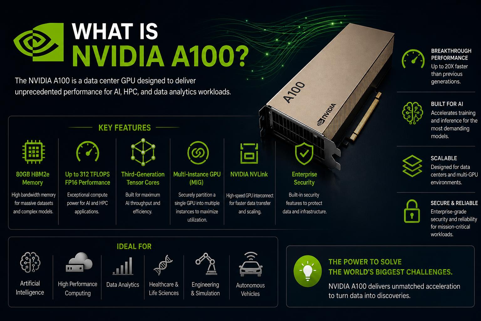
- The NVIDIA A100 GPU delivers cutting-edge performance for AI, HPC, and data analytics through advanced architecture and memory technologies.
- It dramatically accelerates machine learning and deep learning workloads, supporting industry-standard frameworks with robust scalability.
- Key specifications include 6912 CUDA cores, 432 Tensor Cores, and up to 80GB HBM2 memory, all tailored for data centers.
If you are involved in AI, scientific research, or high-performance computing, you’ve no doubt heard about the NVIDIA A100. This GPU isn’t just another graphics card—it’s a technological leap designed to power the world’s most demanding workloads. Whether you’re building conversational AI models or crunching astronomical data sets, the A100 has quickly become a go-to solution across industries for its sheer performance and flexibility.
But with specs lists longer than your arm and marketing buzzwords flying around, what exactly makes the A100 stand out? In this article, we’ll break down everything you need to know about the NVIDIA A100, drawing from the latest official resources, technical sheets, and deep dives, all reframed in plain English. Expect details, caveats, use cases, and even some under-the-hood insights you won’t find on your average comparison chart.
What is the NVIDIA A100?
The NVIDIA A100 is a graphics processing unit (GPU) developed specifically for data centers, AI training, high performance computing (HPC), and advanced analytics workloads. Unveiled in June 2020, it is part of NVIDIA’s Ampere architecture and is considered the flagship solution for enterprise-level acceleration in machine learning, deep learning, and scientific simulation.
Unlike typical gaming GPUs, the A100 is tailored for servers and massive data centers. It’s not designed to connect to a display but rather to drive the performance behind the scenes, managing immense calculations that are crucial for developing AI models, performing deep learning training, running simulations, and crunching big data analytics.
Why Did NVIDIA Create the A100?
AI models have exploded in complexity in recent years, especially with the boom in conversational AI, natural language processing, and recommendation systems. Solving these new challenges demands a dramatic leap in computational power and more efficient scaling of hardware. The previous generation (based on the Volta architecture) was already impressive, but the A100 boosts performance up to 20 times over Volta using its new design, allowing data scientists and researchers to innovate at unprecedented speeds.
Main Features and Specifications
GPU Architecture and Compute Power
- Architecture: Ampere (GA100 core)
- CUDA Cores: 6912
- Tensor Cores: 432 (3rd generation)
- Base/Boost Frequency: 765 MHz / 1410 MHz
- Process Technology: 7nm (chip with 54.2 billion transistors and a die area of 826 mm²!)
The A100’s tensor cores are built for deep learning. They support the latest numeric formats (TF32 for seamless high-speed AI training, as well as BF16, FP16, FP32, FP64, INT4, and INT8 for different model types and workloads), making the GPU extremely adaptable for both accuracy and speed.
Memory
- Memory Size: 40 GB or 80 GB HBM2 (High Bandwidth Memory)
- Memory Bus: 5120-bit width
- Bandwidth: 1.56 TB/s
- L1 Cache: 192 KB per SM
- L2 Cache: 40 MB
For massive data tables and deep learning recommendation models (DLRM), the A100 80GB version achieves up to 1.3TB of unified memory per node—absolutely crucial for training the largest models, where RAM size often becomes the bottleneck.
Connectivity and Scalability
- PCIe Gen 4.0 x16 Interface
- NVIDIA NVLink, NVSwitch for multi-GPU scaling
- 8-pin EPS power connector, max draw 250W
Connectivity options help you scale the A100 across many servers or racks, making it possible to solve enormous problems in minutes that would take days on lesser hardware. For example, 2,048 A100 GPUs have been used to train the BERT large language model at a computing speed that sets industry records.
Physical and Board Design
- Dual-slot card design
- Dimensions: 267 mm (length) x 111 mm (height)
- Recommended system PSU: 600 W
- No video outputs—strictly for compute workloads
The card is designed for servers and not for connecting monitors or direct visualization. Its entire focus is raw compute.
Performance: What Makes the A100 Special?
The A100 doesn’t just crush benchmarks—it redefines them. Let’s look closely at theoretical and real-world figures.
Theoretical Performance
- FP16 (Half Precision): Up to 77.97 TFLOPS
- FP32 (Single Precision): 19.49 TFLOPS
- FP64 (Double Precision): 9.746 TFLOPS
- Tensor Operations (Matrix Cores):
— INT4: 1247.5 TOPS
— INT8: 623.7 TOPS
— FP16/BF16: 311.9 TFLOPS
— TF32: 155.9 TFLOPS
Matrix multiplication is the backbone of AI and deep learning, and the A100’s architecture is purpose-built to speed up those calculations. Its Tensor Cores are specially designed to accelerate AI workloads while maintaining high accuracy and flexible data type support.
Scaling to Massive Systems
The A100 is routinely deployed in clusters, interconnected with NVLink and NVSwitch, allowing researchers to pair thousands of GPUs for distributed training. This is where the A100 shines—training previously unmanageable models in record time and setting industry-leading standards such as those found in MLPerf benchmarks.
Efficiency and Power Consumption
With a TDP of just 250W, the A100 is surprisingly efficient considering its muscle. This allows organizations to pack more power into their data centers without jumping through hoops to manage cooling and power delivery.
Software and Framework Support
The A100 isn’t just powerful hardware—it’s backed by a rich software ecosystem. It supports:
- CUDA 8.0
- OpenCL 3.0
- All major deep learning frameworks (TensorFlow, PyTorch, MXNet, etc.)
- Industry SDKs, such as NVIDIA Magnum IO, for streamlined GPU management and data throughput
The hardware is only as good as the software it runs, so NVIDIA invests heavily in providing up-to-date drivers, containerization via NGC, and continued improvements for popular libraries. The A100 accelerates more than 700 HPC applications and plays nicely with all major deep learning environments right out of the box.
Use Cases: Where the A100 Truly Shines
While the NVIDIA A100 was designed for versatility, several categories of tasks get the most dramatic benefit:
- Deep Learning Training: Models such as BERT, GPT, and DLRM are now trainable at absurd speeds—even models with trillions of parameters.
- AI Inference at Scale: High volume, low-latency inference applications like real-time translation, speech recognition, and recommendation engine serve billions of users across platforms.
- Scientific Computing: Weather modeling, genetics, quantum simulations, and fluid dynamics are performed orders-of-magnitude faster.
- Data Analytics: Real-time analytics and big data processing in fields ranging from finance to genomics.
Organizations everywhere—cloud providers, research centers, startups, and major internet companies—deploy the A100 to tackle workloads unthinkable just a few years ago.
Memory Configuration: 40GB vs 80GB Cards
The A100 comes primarily in two flavors: PCIe 40GB and SXM/PCIe 80GB variants. The larger memory on the 80GB version is especially essential for recommendation systems, large language models, and data science applications dealing with massive data tables. Unified memory approaches 1.3TB per node in multi-GPU configurations, allowing unprecedented model and dataset sizes to be used without slowdowns due to memory bottlenecking.
Hardware Breakdown: Under the Hood of the A100
- Shading Units: 6912
- Texture Mapping Units (TMUs): 432
- ROPs: 160
- SM Count: 108
This massive parallelization is the secret sauce for the incredible processing throughput the A100 can offer—not just for floating point calculations, but for tensor operations critical to modern neural networks.
Industry Recognition and Benchmarks
The A100’s dominance is not just theoretical. It has regularly set records in MLPerf, the gold standard for AI performance benchmarking. Whether in training speed or inference throughput, the A100 frequently tops the charts, proving its value in both academic and commercial environments. See official MLPerf results for up-to-date data and challenge results.
Deployment: Where Can You Find the A100?
The A100 is available in multiple form factors—from PCIe cards that fit into standard servers, to SXM4 modules intended for high-density data center racks. You’ll also find these GPUs in virtually all major public cloud providers, via GPU-equipped virtual machines and AI platforms.
Leading server vendors like PNY and Leadtek offer reference and customized designs based on the A100 for solutions ranging from entry-level AI research to enterprise-grade, mission-critical deployments.
Compatibility and Limitations
Not every workload can make full use of an A100—you’ll need PCIe 4.0 support, robust cooling, and an adequate power supply. And, despite its raw power, the A100 does not support gaming APIs like DirectX or OpenGL, as its design is purely compute-focused. There are also no display outputs on the card, reinforcing its role as a backend workhorse.
Recent Changes and Lifecycle
As of its introduction, the A100 replaced earlier server GPUs like the Tesla Turing and leads to future upgrades such as the Server Ada series. The production status for A100 is ‘End-of-life’ in some SKUs, but driver and software support remains active, ensuring current deployments remain viable for years to come.
Why Does This Matter for Industries?
Simply put, massive leaps in model size and training speed have spurred innovation everywhere—from instant translation technologies to genomics, clean energy modeling, and automated driving. The A100 plays a pivotal role in making these advancements both technologically and economically feasible by dramatically slashing training times and unlocking new scientific horizons.
Further Resources
To see official technical details, whitepapers, and data sheets, visit the NVIDIA A100 official product page, Ampere Architecture Whitepaper (PDF), and the A100 Datasheet (PDF). For GPU specification and in-depth comparisons, you can also explore resources like TechPowerUp.
Summing up, the NVIDIA A100 has changed the landscape for artificial intelligence and high-performance computing by setting new records, delivering flexible scalability, and making tasks feasible that were once out of reach for even the best-equipped research teams. Its robust combination of hardware innovation and software ecosystem support makes it not just a performance leader, but a vital tool powering the AI revolution across industries.