
- The 555 timer IC stands as one of the most influential and versatile integrated circuits in electronics.
- Understanding its pinout, internal design, and core functionality is essential to mastering both basic and advanced circuits.
- Every operational mode—astable, monostable, and bistable—unlocks unique applications, from simple blinkers to sophisticated analog and digital uses.
- Modern circuit design benefits from a deep dive into derivative chips, specification differences, and common pitfalls when working with the 555 timer.
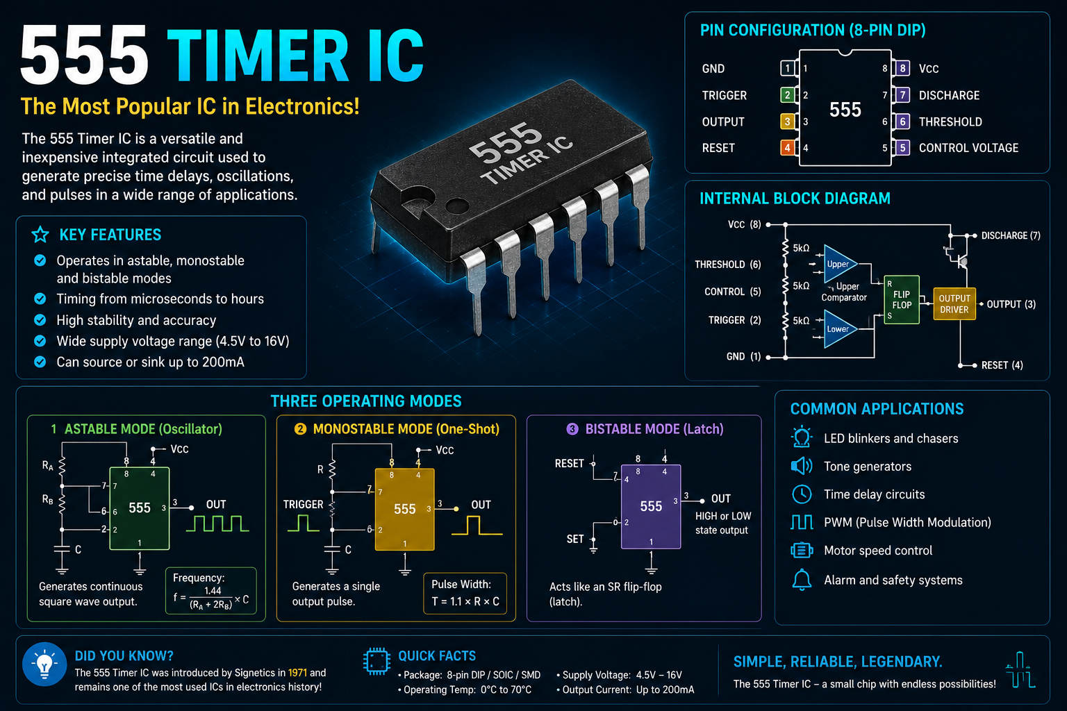
Few electronic components have reached the iconic status of the 555 timer IC. Whether you’re just starting out with breadboards or are an old pro building complex analog circuits, odds are you’ve come across this small but mighty chip. Created in the early 1970s, the 555 timer wasn’t just another IC—it became the Swiss Army knife for hobbyists and engineers alike, finding its way into thousands of applications, kits, and devices. Its ongoing popularity isn’t just nostalgia: the 555 timer remains an essential tool for creating anything from blinking LEDs and alarm buzzers to PWM motor controls and modular synths.
This in-depth guide is designed to go way beyond the basics. We’re diving deep into every facet of the 555 timer: its history, the meaning behind its quirky name, the anatomy of its pinout, what actually happens inside the chip, and how its various operating modes allow you to pull off a remarkable range of clever circuits. If you’re ready for more than just a datasheet summary, keep reading to unlock everything you need to know about the 555 timer IC.
The 555 Timer IC at a Glance: What Makes It Special?
The 555 timer—often just called “the 555″—is an integrated circuit designed for timing, pulse generation, and oscillator applications. First hitting the market in 1972 under the Signetics NE555 part number, this chip stood out for its combination of flexibility, affordability, and ease of use. Unlike more complex programmable chips, the 555’s brilliance lies in how you can turn a handful of resistors and capacitors into various clever timers, oscillators, and triggers.
- Versatile operating modes (astable, monostable, bistable, Schmitt trigger)
- Robust output current of up to 200 mA (good for driving loads such as LEDs, buzzers, and relays directly)
- Minimal external components required to create fascinating behaviors
- Available in single (NE555), dual (NE556), and quad (NE558) configurations
A Brief History: The Inventor and the Launch of the 555 Timer
Hans Camenzind was the man behind the magic of the 555 timer. Working under contract for Signetics in 1971, he developed the 555 as a way to create a universal timing circuit by drawing on his previous work with oscillators for phase-locked loops. Faced with an unstable economy and rounds of layoffs at Signetics, Camenzind continued developing the idea of a general-purpose chip. Although some colleagues believed its functionality could be assembled using existing components, Camenzind’s elegant approach convinced the Signetics marketing manager.
The chip quickly conquered the market. By 1972, twelve companies were producing their own versions, and Camenzind later noted that “nine out of ten” uses of the chip turned out to be things he had never imagined. Its simple design—which condensed the required circuitry into eight pins instead of the originally planned 14—and the use of inexpensive bipolar transistors helped drive its popularity.
Understanding the 555 Timer Pinout
Getting the most out of the 555 timer starts with understanding what every pin does. It comes in a standard 8-pin Dual In-line Package (DIP-8), and while many pinout diagrams are available, here’s a breakdown with some extra insight:
- Pin 1 – Ground: This is the ground reference for the chip (0V).
- Pin 2 – Trigger: When the voltage here drops below 1/3 of VCC, it causes the output to go high, starting or resetting the timing interval.
- Pin 3 – Output: The output pin delivers either a high or low voltage. The chip can sink or source 100–200 mA—always check the specific datasheet—allowing direct connection to typical LEDs, buzzers, or relays.
- Pin 4 – Reset: This is an active-low pin—pulling it to ground resets the timer and makes the output go low. If you don’t need the reset feature, tie the reset pin high to prevent accidental resets caused by electrical noise.
- Pin 5 – Control Voltage: Usually left unused, this pin allows external control of the reference threshold voltage. A 0.01 μF (10 nF) capacitor to ground is often added to filter out noise. If your circuit is misbehaving, try adding this capacitor—it can help stabilize it.
- Pin 6 – Threshold: When this pin’s voltage rises above 2/3 of VCC, it causes the output to go low, ending the timing interval.
- Pin 7 – Discharge: This pin connects internally to an open-collector transistor—or an open-drain transistor in CMOS versions—that grounds the capacitor during certain parts of the timing cycle. It is used to reset the timing capacitor in astable and monostable modes.
- Pin 8 – VCC (Supply): Connect this pin to the positive voltage source, usually 4.5 to 16V for bipolar chips and sometimes 2–15V for CMOS versions.
Want an even more detailed breakdown? For direct datasheet references and additional visuals, visit build-electronic-circuits.com.
Inside the 555: How It Operates and What’s Happening on the Silicon
What makes the 555 timer tick inside its black plastic case? The original design fits around 25 transistors, 2 diodes, and 15 resistors onto a silicon chip. Its internal structure combines a voltage divider network, two comparators, a flip-flop (SR latch), an open-collector discharge transistor, and a push-pull output stage.
- Voltage Divider (3 × 5kΩ resistors in bipolar chips) splits the supply voltage, establishing reference voltages at 1/3 and 2/3 of VCC for the comparator inputs.
- Threshold Comparator monitors Pin 6 and triggers when this input exceeds 2/3 of VCC, resetting the output.
- Trigger Comparator checks Pin 2 and sets the output high when the voltage falls below 1/3 of VCC.
- SR Latch stores the result of the comparators, determining the overall output state.
- Reset (Pin 4) can force the output low at any time, overriding the comparators.
- Discharge Transistor (Pin 7) grounds the connected capacitor during the low part of the cycle.
- Output Stage (Pin 3) can source or sink significant current, enough to operate small loads without an external transistor.
Variants of the 555, such as the NE555 and SE555, offer different performance characteristics, including commercial- and military-grade temperature ranges. Lower-power CMOS versions, such as the ICM7555, TLC555, and LMC555, are ideal for battery-powered circuits. Dual and quad versions—the 556 and 558—fit multiple timers into a single chip, with the 556 essentially being a dual 555 and the 558 a quad timer with some reduced features and shared pins.
Operating Modes: How to Use the 555 Timer in Your Circuits
The 555 timer is famous not just for what it is, but for what it allows you to do. Each operating mode unlocks unique creative possibilities:
Astable Mode: Making Oscillators and Blinking Lights
Astable means “not stable.” In this configuration, the 555 continuously switches its output back and forth, turning it into a simple electronic oscillator. This mode is the foundation for blinking LEDs, generating sounds, flashing lamps, and much more.
To set it up, connect two resistors (R1 and R2) and a capacitor (C), as shown in most 555 astable-mode schematics. The discharge and threshold pins are both connected to the capacitor, allowing the 555 to charge and discharge it repeatedly. As the voltage across the capacitor cycles between 1/3 and 2/3 of VCC, the output switches between high and low, generating a square or rectangular wave. To better understand how it works, you can learn more about duty-cycle modulation techniques using the 555 timer in this guide to pulse-width modulation (PWM).
- Applications: Clock pulses for digital circuits, light flashers, sound-effect generators, simple PWM circuits, and periodic timers
- Component selection: Adjust the resistor and capacitor values to control the pulse interval. For specialized duty cycles, such as a shorter high time than low time, add a diode across R2.
If you want to get super-precise: Use the formulas below to calculate the timing values in astable mode:
Low time: tlow = ln(2) × R2 × C
Frequency: f = 1 / (ln(2) × (R1 + 2 × R2) × C)
Duty cycle (%): D = ((R1 + R2)/(R1 + 2 × R2)) × 100
Monostable Mode: One-Shots, Alarms, and Delayed Switches
Monostable means “only one stable state.” In this configuration, the 555 remains idle with its output low until it receives a trigger pulse. When triggered, the output goes high and remains high for an interval determined by an external resistor and capacitor. It then returns low, regardless of what happens at the input afterward.
- Applications: Push-button timers, touch-sensitive alarms, frequency dividers, switch-debouncing circuits, and triggered buzzers
- Real-world example: An LED that remains lit for several seconds after a button is pressed. The chip automatically turns it off after the set interval. Miniature alarms and adjustable timers often use this circuit.
The timing interval formula for monostable mode is:
The output remains high for this amount of time, regardless of how long the trigger input stays low. Subsequent triggers are ignored until the timing interval has finished.
Bistable Mode: Flip-Flops for ON/OFF Control
Bistable means “two stable states.” In this configuration, the 555 works as a simple flip-flop or memory circuit. By separately activating the trigger and threshold pins, you can switch the output between high and low, allowing you to build circuits in which one button turns a lamp on and another turns it off.
- Applications: Push-button ON/OFF toggle switches, basic logic memory, and latched alarm states
- Hobby project example: Add separate ON and OFF buttons using push buttons and pull-up resistors to latch an LED’s state with the 555. The chip holds the output until the opposite button is pressed.
Schmitt Trigger (Inverter) Mode: Cleaning Up Noisy Signals
Finally, the 555 can convert a messy, noisy analog signal into a clean digital one. By connecting both the threshold and trigger inputs to the incoming signal—centered at 1/2 VCC using a voltage divider—the chip adds hysteresis. This provides immunity to small voltage fluctuations and converts slow or noisy inputs, such as those from a mechanical switch, into sharp, clean transitions.
- Applications: Emergency-stop circuits, conditioning noisy sensor signals, and creating sharp pulses from variable analog inputs
Real-World Circuit Examples: Blinking LEDs, Alarms, Motors, and More
The real magic of the 555 timer becomes apparent through its countless applications. Here are a few hands-on projects and their corresponding configurations:
LED Flasher (Astable)
- 9V power supply
- NE555 with a pair of 1kΩ resistors and a 1000 μF capacitor
- The LED flashes approximately once every two seconds, making it ideal as a visual indicator or simple lighting effect
For a simple build, check out the instructions at .
One-Shot Alarm (Monostable)
- 9V power supply
- NE555 configured with an external trigger button
- The output drives an LED or buzzer for a timed interval, such as 10 seconds
- Changing the timing resistor or capacitor alters how long the output remains active
Push-Button Flip-Flop (Bistable)
- Two push buttons used as separate ON and OFF controls
- Pull-up resistors keep the inputs high when inactive
- The output controls an LED, relay, or another low-power device, with each button selecting a different state
Motor and High-Load Drivers
The 555 can source or sink up to 200 mA directly. If you need more power for motors, large LED arrays, lamps, or similar loads, connect the output to the base of an NPN transistor through a resistor—around 1kΩ is a reasonable starting value. When using MOSFETs, choose logic-level models that are compatible with the timer’s output voltage.
DIY Siren and Flashing Lights (Astable, Dual LEDs)
- Configure sourcing and sinking outputs to alternately flash blue and red LEDs, making them ideal for toy sirens or model emergency vehicles
- Adjust the resistor and capacitor values to change the flashing speed and pattern
Common 555 Mistakes and Pro Tips
- Always use a 10 nF decoupling capacitor on Pin 5, especially in noisy or unreliable circuits.
- Tie the reset pin high to VCC if you are not using it. Never leave it floating.
- Be mindful of the maximum current: Do not drive power-hungry loads directly. Use a transistor instead.
- Double-check your resistor and capacitor values—incorrect values are one of the most common causes of timing errors.
- Pay attention to logic levels on the trigger and threshold pins, especially when using supply voltages below 9V or long wires that may pick up electrical noise.
Package Types and Variations: More Than Just an 8-Pin Chip
Although the DIP-8 package is the most famous, the 555 timer has appeared in several different forms over the years:
- DIP-8 or TO-5-8: Classic single-timer ICs such as the NE555 and SE555
- DIP-14: NE556, a dual 555 timer containing two timing circuits in one chip and sharing the power and ground pins
- DIP-16: NE558 and NE559 quad timers, with minor functionality reductions for each timer
- SO-8, SO-14, SSOP-8, TSSOP-8, VSSOP-8, and even BGA packages for surface-mount and miniaturized applications
- SOT23-5: MIC1555, an ultra-compact version for SMD designs
Choosing the right variant matters when designing for extreme temperatures or low-power operation. CMOS variants offer dramatically lower standby current—sometimes only a few tens of microamps—making them ideal for coin-cell and long-life battery-powered projects.
Diving Deeper: The 555’s Internal Schematic and How It All Works
Here’s a closer look under the hood, matching each key functional block:
- Voltage Divider: The backbone of the circuit. By dividing the supply voltage into thirds using three resistors in a standard bipolar chip, it establishes the reference thresholds for the two comparators.
- Comparators: Two analog comparators monitor the trigger input—Pin 2, the lower threshold—and the threshold input—Pin 6, the upper threshold.
- Latch (SR Flip-Flop): Holds the output state and only changes when activated by the comparator logic or by Pin 4, the reset input.
- Output Stage: A high-current totem-pole driver follows the latch and can source loads of up to 200 mA or sink similar amounts when the output is low.
- Discharge Transistor: Grounds the timing capacitor at the appropriate moments, controlling oscillation periods or timing delays depending on the circuit configuration.
Pin Descriptions and Special Considerations
| Pin | Name | Direction | Main Function |
|---|---|---|---|
| 1 | GND | Power | Ground reference voltage (0V) |
| 2 | Trigger | Input | Activates the timer when the voltage falls below 1/3 of VCC |
| 3 | Output | Output | Push-pull output that goes high or low depending on the internal logic |
| 4 | Reset | Input | Forces the output low; tie it high if unused |
| 5 | Control | Input | An external voltage sets the timing thresholds; it is usually decoupled with a 10 nF capacitor |
| 6 | Threshold | Input | Ends the timing interval when the voltage exceeds 2/3 of VCC |
| 7 | Discharge | Open Collector | Electrically grounds the timing capacitor |
| 8 | VCC | Power | Supply voltage, typically 2–18V depending on the device type |
Advanced Modes: PWM, Frequency Adjustment, and Beyond
Pulse-width modulation (PWM) with the 555 is widely used because it makes it possible to control motor speed, adjust LED brightness, and generate analog-like outputs from digital signals. Duty-cycle modulation can be achieved by adjusting the voltage applied to the control-voltage input (Pin 5), which can be used to introduce dynamic variations and create power-control circuits and analog simulations with the 555 timer.
Switch-mode power supplies and voltage regulation have also been implemented using the 555 to build PWM-controlled power supplies, allowing the output to be adjusted precisely according to specific requirements.
Typical Specifications: Know Your 555 Limits
| Specification | NE555 Bipolar |
|---|---|
| Supply Voltage (VCC) | 4.5–16 V |
| Supply Current at 5 V | 3–6 mA |
| Maximum Output Current | 200 mA |
| Minimum Power Consumption | 30 mW |
| Maximum Power Consumption | 600 mW |
| Operating Temperature | 0°C to +70°C for the NE555; -55°C to +125°C for the military-grade SE555 |
For CMOS versions, power consumption and output-current limitations may vary. These devices also offer advantages such as lower power consumption and a wider operating-voltage range. You can consult the Texas Instruments LM555 datasheet for detailed comparisons and specifications.
Popular Derivatives: NE555, NE556, NE558, and CMOS Alternatives
The 555 has been produced in many different versions and packages over the years, adapting to a wide range of applications and requirements:
- NE555: The classic version, commonly supplied in a DIP-8 package and widely used in general-purpose circuits.
- NE556: Two 555 timers in a single chip, saving space in compact designs.
- NE558/NE559: Four timers in a single package, using simplified internal components.
- CMOS versions such as the TLC555 and ICM7555: Low-power devices ideal for portable and low-voltage applications.
Differences in Specifications and Manufacturer Notes
Pinout and Package Comparison for Dual and Quad Timers
| Pin Number | Single 555 | Dual 556 | Pin Name | Description |
|---|---|---|---|---|
| 1 | 1 | 7/7 | Ground | Ground reference (0V) |
| 2 | 2 | 6/8 | Trigger | Input pulse that starts the timing interval |
| 3 | 3 | 5/9 | Output | High or low output depending on the operating mode |
| 4 | 4 | 4/10 | Reset | Forces the output low; connect it to VCC when unused |
| 5 | 5 | 3/11 | Control Voltage | External reference voltage, usually connected to a 10 nF capacitor |
| 6 | 6 | 2/12 | Threshold | Ends the timing interval when the voltage exceeds 2/3 of VCC |
| 7 | 7 | 1/13 | Discharge | Usually connects the timing capacitor to ground in astable and monostable modes |
| 8 | 8 | 14 | VCC | Positive supply voltage |
Design and Component Tips for Your 555 Projects
- Combine multiple 555 timers: Use dual or quad versions for sequencing circuits, tone generators, or mixed analog and digital applications.
- Use the control pin for voltage-controlled oscillators: Apply a modulation voltage for analog synthesizers, dynamic adjustments, or frequency control in configurations such as PWM circuits.
- Add a diode in parallel with R2 in astable mode to achieve duty cycles below 50%, which can be important for particular effects and timing requirements.
- For long delays: Use high-value electrolytic capacitors and high-value resistors while taking component stability and leakage into account.
- To interface the 555 with logic circuits: Configure it as a Schmitt trigger to eliminate noise and debounce electronic controls.
The Current State of the 555: Why Is It Still Popular?
Although microcontrollers and programmable devices now dominate many applications, the 555 remains highly relevant. It is easier, cheaper, and more reliable for basic timing or pulse-generation tasks in resource-limited projects and rapid prototypes. Its lasting popularity is also due to:
- Widespread availability: Almost every electronic-component supplier stocks at least one version of the NE555.
- Affordable price: It is inexpensive enough to experiment with without worrying too much about damaging it.
- Educational value: It is a practical tool for learning analog and digital circuit concepts before moving on to microcontrollers.
Online resources such as , YouTube tutorials, and advanced application notes from manufacturers continue to keep knowledge about the chip and its uses alive.
Further Exploration: Books, Datasheets, and Learning Resources
- “555 Timer Applications Sourcebook With Experiments” by Howard Berlin: Practical circuits
- “IC Timer Cookbook” by Walt Jung: A classic reference for timer-based circuit design
- “Timer/Generator Circuits Manual” by R.M. Marston
- “Designing Analog Chips” by Hans Camenzind: A guide to understanding the analog-design mindset behind the 555
- Official datasheets from Texas Instruments, ON Semiconductor, Renesas, and other manufacturers
Don’t forget online resources such as Digi-Key’s 555 Timer Calculator and circuit schematics that can help accelerate your experimentation.
The enduring interest in the 555 is no coincidence. It is a perfect combination of ingenious engineering, practical flexibility, and constant accessibility. Whether it is lighting an LED or automating a process, this chip offers an unbeatable balance between function and fun.
Pulse-Width Modulation (PWM): A Complete Guide to Digital Power Control